【ug572】UltraScale体系结构时钟资源手册节选
概述
时钟架构概述
The UltraScale architecture clocking resources manage complex and simple clocking requirements with dedicated global clocks distributed on clock routing and clock distribution resources. The clock management tiles (CMTs) provide clock frequency synthesis, deskew, and jitter filtering functionality. Non-clock resources such as local routing are not recommended when designing for clock functions.
UltraScale体系结构时钟资源通过分布在时钟布线和时钟分布资源上的专用全局时钟来管理复杂和简单的时钟要求。时钟管理区块(CMTs)提供时钟频率合成、去偏斜和抖动过滤的功能。在设计时钟功能时,不建议使用非时钟资源,如本地布线资源。
-
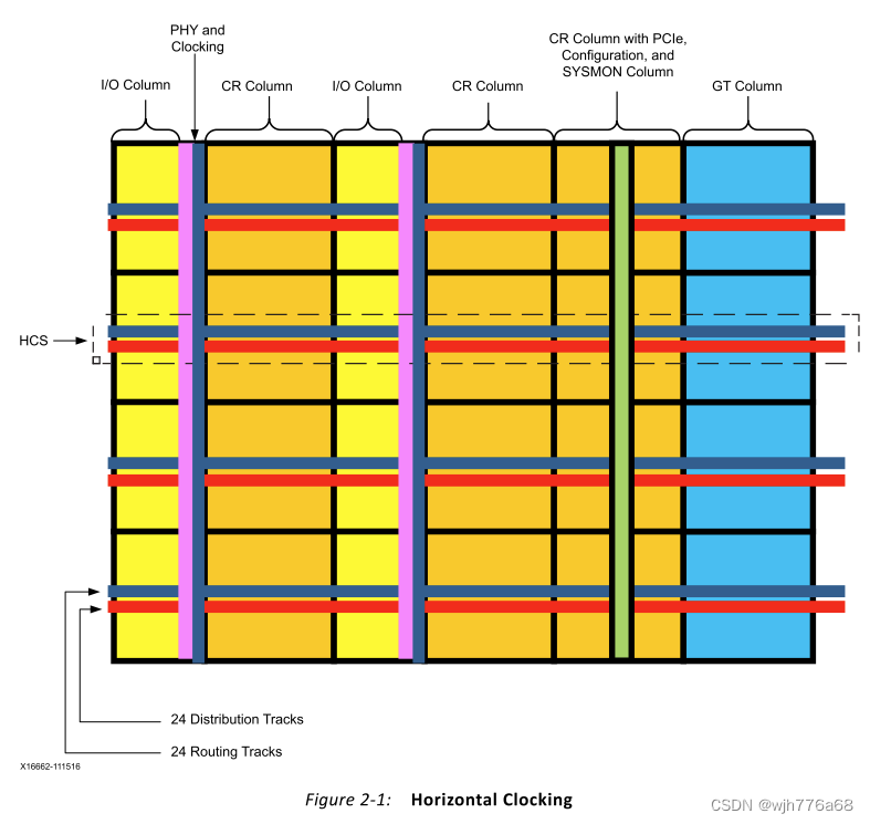
The device is subdivided into columns and rows of segmented clock regions (CRs). CRs differ from previous families because they are arranged in tiles and do not span half the width of a device. A CR contains configurable logic blocks (CLBs), DSP slices, block RAMs, interconnect, and associated clocking. The height of a CR is 60 CLBs, 24 DSP slices, and 12 block RAMs with a horizontal clock spine (HCS) at its center. The HCS contains the horizontal routing and distribution resources, leaf clock buffers, clock network interconnections, and the root of the clock network. Clock buffers drive directly into the HCS. There are 52 I/Os per bank and four gigabit transceivers (GTs) that are pitch matched to the CRs. A core column contains configuration, System Monitor (SYSMON), and PCIe? blocks to complete a basic device.
-
Ultrascale设备被细分为由行列构成的分片时钟区域(CRs)。CRs与以前的FPGA系列不同,Ultrascale的CR排列在区块中,跨度不再是设备宽度的一半。一个CR包含可配置逻辑块(CLBs)、DSP、BRAM、互连和相关时钟。一个CR的高度等价于60个CLB或24个DSP或12个BRAM,CR中心有一个水平时钟脊线(HCS)。HCS包含水平路由和分配资源、叶时钟缓冲区、时钟网络互联和时钟网络的根。时钟缓冲器直接驱动到HCS。一个bank的52个I/O和4个GT收发器(GTs),它们与CRs的间距匹配。核心列包含配置、系统监视器(SYSMON)和PCIe?模块用于实现一个基本设备。
-
Adjacent to the input/output block columns are the physical layer (PHY) blocks with CMTs, global clock buffers, global clock multiplexing structures, and I/O logic management functions. The clocking drives vertical and horizontal connectivity through separate clock routing and clock distribution resources via HCS into the CRs and I/Os.
-
与输入/输出块列相邻的是具有CMTs、全局时钟缓冲器、全局时钟多路复用结构和I/O逻辑管理功能的物理层(PHY)块。驱动垂直和水平连接的时钟通过单独的时钟布线和时钟分配资源通过HCS进入CR和I/O。
-
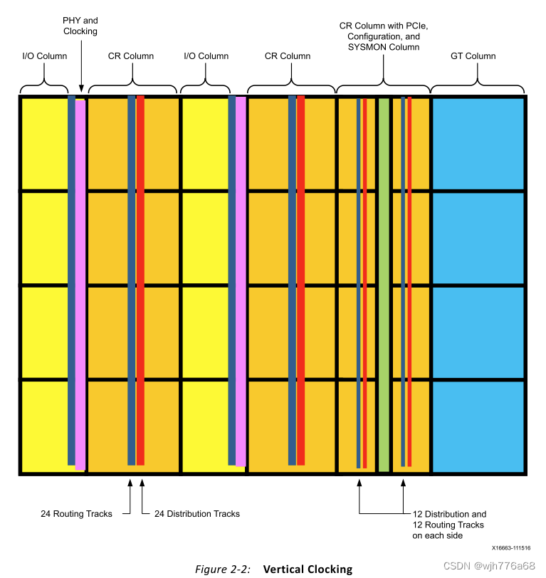
Horizontal clock routing and distribution tracks drive horizontally into the CRs. Vertical routing and distribution tracks drive vertically adjacent CRs. The tracks are segmentable at the CR boundaries in both the horizontal and vertical directions. This allows for the creation of device-wide global clocks or local clocks of variable size.
-
水平时钟布线和水平分配轨道横向驱动进入CRS。垂直时钟布线和垂直分配轨道垂直驱动相邻的CR。轨道在水平和垂直方向上都可在CR边界处分段。这允许设备范围的全局时钟或可变大小的本地时钟两种方式的构造。
-
The distribution tracks drive the clocking of synchronous elements across the device. Distribution tracks are driven by routing tracks or directly by the clocking structures in the PHY.
-
分配轨道驱动设备上同步元件的时钟。分配轨道由布线轨道或直接由硬件上的时钟结构驱动。
-
I/Os are directly driven from the PHY clocking and/or an adjacent PHY via routing tracks.
-
I/O直接从硬件上的时钟和/或通过布线轨道相邻的硬件驱动。
-
A CMT contains one mixed-mode clock manager (MMCM) and two phase-locked loops (PLLs).
-
CMT包含一个混合模式时钟管理器(MMCM)和两个锁相环(PLL)。
时钟布线资源概述
Each I/O bank contains global clock input pins to bring user clocks onto the device clock management and routing resources. The global clock inputs bring user clocks onto:
每个 I/O Bank 都包含全局时钟输入引脚,可将用户时钟引入器件时钟管理和布线资源。全局时钟输入将用户时钟带到:
-
Clock buffers in the PHY adjacent to the same bank
-
PHY 中与同一bank相邻的时钟缓冲器
-
CMTs in the PHY adjacent to the same bank
-
PHY 中与同一bank相邻的 CMTs
Each device has three global clock buffers: BUFGCTRL, BUFGCE, and BUFGCE_DIV. In addition, there is a local BUFCE_LEAF clock buffer for driving leaf clocks from horizontal distribution to various blocks in the device. BUFGCTRL has derivative software representations of types BUFGMUX, BUFGMUX1, BUFGMUX_CTRL, and BUFGCE_1. BUFGCE is for glitchless clock gating and has software derivative BUFG (BUFGCE with clock enable tied High). The global clock buffers drive routing and distribution tracks into the device logic via HCS rows. There are 24 routing and 24 distribution tracks in each HCS row. There is also a BUFG_GT that generates divided clocks for GT clocking. The clock buffers:
每个器件都有三个全局时钟缓冲区:BUFGCTRL、BUFGCE 和 BUFGCE_DIV。此外,还有一个本地 BUFCE_LEAF 时钟缓冲区,用于驱动叶时钟从水平分布到器件中的各个模块。 BUFGCTRL 具有 BUFGMUX、BUFGMUX1、BUFGMUX_CTRL 和 BUFGCE_1 类型的派生软件表示形式。 BUFGCE 用于无毛刺时钟门控,并具有软件衍生 BUFG(时钟使能连接为高电平的 BUFGCE)。全局时钟缓冲器通过 HCS 行将布线和分配轨道驱动到器件逻辑中。每个 HCS 行中有 24 个路由轨道和 24 个分配轨道。还有一个 BUFG_GT 为 GT 时钟生成分频时钟。这些时钟缓冲器:
-
Can be used as a clock enable circuit to enable or disable clocks either globally, locally, or within a CR for fine-grained power control.
-
可用作时钟使能电路,以全局、本地或 CR 内启用或禁用时钟,以实现细粒度功率控制。
-
Can be used as a glitch-free multiplexer to:
-
可用作无毛刺多路复用器:
-
select between two clock sources.
-
在两个时钟源之间进行选择。
-
switch away from a failed clock source.
-
切换以不再使用发生故障的时钟源。
-
-
Are often driven by a CMT to:
-
通常由 CMT 推动:
-
eliminate the clock distribution delay.
-
消除时钟分配延迟。
-
adjust clock delay relative to another clock.
-
调整相对于另一个时钟的时钟延迟。
-
CMT概述
Each device has a CMT as part of the PHY next to each of the I/O banks. A CMT consists of one MMCM and two PLLs. The MMCM is the primary block for frequency synthesis for a wide range of frequencies, and serves as a jitter filter for either external or internal clocks, and deskew clocks among a wide range of other functions. The PLL’s primary purpose is to provide clocking to the PHY I/Os, but can also be used for clocking other resources in the device in a limited fashion. The device clock input connectivity allows multiple resources to provide the reference clock(s) to the MMCM and PLL.
每个设备在每个 I/O Bank 旁边都有一个 CMT作为 PHY 的一部分。一个 CMT 由一个 MMCM 和两个 PLL 组成。 MMCM 具有大范围的可调频率,是各种频率合成的主要模块,可用作外部或内部时钟的抖动滤波器,以及各种其他功能中的抗偏移时钟。 PLL 的主要用途是为 PHY I/O 提供时钟,但也可用于以有限的方式为器件中的其他资源提供时钟。器件时钟输入连接允许多个资源向 MMCM 和 PLL 提供参考时钟。
MMCMs have infinite fine phase shift capability in either direction and can be used in dynamic phase shift mode. MMCMs also have a fractional counter in either the feedback path or in one output path, enabling further granularity of frequency synthesis capabilities.
MMCM 在任一方向都具有无限精细的相位偏移能力,并且可用于动态相移模式。 MMCM 还在反馈路径或一个输出路径中具有小数计数器,从而实现了频率合成功能的进一步粒度。
The LogiCORE? IP clocking wizard is available to assist in utilizing MMCMs and PLLs to create clock networks in UltraScale architecture designs. The GUI interface is used to collect clock network parameters. The clocking wizard chooses the appropriate CMT resource and optimally configures the CMT resource and associated clock routing resources.
LogiCORE? IP 时钟向导可帮助利用 MMCM 和 PLL 在 UltraScale 架构设计中创建时钟网络。 GUI界面用于采集时钟网络参数。时钟向导选择适当的 CMT 资源并优化配置 CMT 资源和关联的时钟路由资源。
与前几代 FPGA 的时钟差异
UltraScale architecture-based devices have significant innovations in the clocking architecture. In general, there is a minimal difference between global and local clock buffers. Thus, the 7 series regional clock buffers have been replaced by new clock buffers with more global reach while automatically utilizing local clock buffers for local distribution of the clocks. The CMT block consists of one MMCM and two PLLs. The MMCM is very similar to the 7 series family while the PLL has new features for the I/O PHY clocking, but a reduced set of functionality and connectivity with respect to clocking the rest of the device.
基于 UltraScale 架构的设备在时钟架构方面具有重大创新。一般来说,全局时钟缓冲器和本地时钟缓冲器之间的差异很小。因此,7 系列区域时钟缓冲器已被具有更大全局覆盖范围的新时钟缓冲器取代,同时自动利用本地时钟缓冲器进行时钟的本地分配。 CMT 模块由一个 MMCM 和两个 PLL 组成。 MMCM 与 7 系列非常相似,而 PLL 具有用于 I/O PHY 时钟的新功能,但与器件其余部分的时钟相关的功能和连接性有所减少。
时钟资源
概述
UltraScale? architecture-based devices have several clock routing resources to support various clocking schemes and requirements, including high fanout, short propagation delay, and extremely low skew. To best utilize the clock routing resources, the designer must understand how to get user clocks from the PCB to the UltraScale devices, decide which clock routing resources are optimal, and then access those clock routing resources by utilizing the appropriate I/O and clock buffers.
基于 UltraScale? 架构的器件具有多种时钟布线资源,可支持各种时钟方案和要求,包括高扇出、短传播延迟和极低偏斜。为了充分利用时钟布线资源,设计人员必须了解如何将用户时钟从 PCB 获取到 UltraScale 器件,确定哪些时钟布线资源是最佳的,然后通过利用适当的 I/O 和时钟缓冲器来访问这些时钟布线资源。
全局时钟输入
External global user clocks must be brought into the UltraScale device on differential clock
pin pairs called global clock (GC) inputs. There are four GC pin pairs in each bank that have
direct access to the global clock buffers, MMCMs, and PLLs that are in the CMT adjacent to
the same I/O bank. The UltraScale+ architecture has four HDGC pins per HD I/O bank. HD
I/O banks are only part of the UltraScale+ family. Since HD I/O banks do not have a XIPHY
and CMT next to them, the HDGC pins can only directly drive BUFGCEs (BUFGs) and not
MMCMs/PLLs. Therefore, clocks that are connected to an HDGC pin can only connect to
MMCMs/PLLs through the BUFGCEs. To avoid a design rule check (DRC) error, set the
property CLOCK_DEDICATED_ROUTE = FALSE. GC inputs provide dedicated, high-speed
access to the internal global and regional clock resources. GC inputs use dedicated routing
and must be used for clock inputs where the timing of various clocking features is
imperative. General-purpose I/O with local interconnects should not be used for clock
signals.
外部全局用户时钟必须通过称为全局时钟 (GC) 输入的差分时钟引脚对引入 UltraScale 器件。每个 Bank 中有四个 GC 引脚对,可以直接访问 CMT 中与同一 I/O Bank 相邻的全局时钟缓冲器、MMCM 和 PLL。 UltraScale+ 架构的每个 HD I/O Bank 有四个 HDGC 引脚。 HD I/O Bank 只是 UltraScale+ 系列的一部分。由于 HD I/O Bank 旁边没有 XIPHY 和 CMT,因此 HDGC 引脚只能直接驱动 BUFGCE (BUFG),而不能驱动 MMCM/PLL。因此,连接到 HDGC 引脚的时钟只能通过 BUFGCE 连接到 MMCM/PLL。要避免设计规则检查 (DRC) 错误,请设置属性 CLOCK_DEDICATED_ROUTE = FALSE。 GC 输入提供对内部全局和区域时钟资源的专用高速访问。 GC 输入使用专用布线,并且必须用于时钟输入,其中各种时钟功能的时序是必不可少的。具有本地互连的通用 I/O 不应用于时钟信号。
Each I/O bank is located in a single clock region and includes 52 I/O pins. Of the 52 I/O pins
in each I/O bank in every I/O column, there are four global clock input pin pairs (a total of
eight pins). Each global clock input:
每个 I/O Bank 位于单个时钟区域并包括 52 个 I/O 引脚。每个 I/O 列的每个 I/O Bank 的 52 个 I/O 引脚中,有 4 个全局时钟输入引脚对(总共 8 个引脚)。每个全局时钟输入:
-
Can be connected to a differential or single-ended clock on the PCB.
-
可连接到 PCB 上的差分或单端时钟。
-
Can be configured for any I/O standard, including differential I/O standards.
-
可针对任何 I/O 标准进行配置,包括差分 I/O 标准。
-
Has a P-side (master), and an N-side (slave).
-
有一个 P 侧(主)和一个 N 侧(从)。
Single-ended clock inputs must be assigned to the P (master) side of the GC input pin pair.
If a single-ended clock is connected to the P-side of a differential clock pin pair, the N-side
cannot be used as another single-ended clock pin—it can only be used as a user I/O.
单端时钟输入必须分配给 GC 输入引脚对的 P(主)侧。如果单端时钟连接到差分时钟引脚对的 P 侧,则 N 侧不能用作另一个单端时钟引脚 - 它只能用作用户 I/O。
GC inputs can be used as regular I/O if not used as clocks. When used as regular I/O, global
clock input pins can be configured as any single-ended or differential I/O standard. GC
inputs can connect to the PHY adjacent to the banks they reside in.
如果不用作时钟,GC 输入可用作常规 I/O。当用作常规 I/O 时,全局时钟输入引脚可配置为任何单端或差分 I/O 标准。 GC 输入可以连接到与其所在bank相邻的 PHY。
字节时钟输入
Byte-lane clock (DBC and QBC) input pin pairs are dedicated clock inputs directly driving
source synchronous clocks to the bit slices in the I/O banks. In memory applications, these
are also known as DQS. When not used for I/O byte clocking these pin have other functions
such as general purpose I/Os.
字节通道时钟(DBC 和 QBC)输入引脚对是专用时钟输入,直接将源同步时钟驱动到 I/O Bank 中的位片。在内存应用中,这些也称为 DQS。当不用于 I/O 字节时钟时,这些引脚具有其他功能,例如通用 I/O。
时钟缓冲器和时钟布线
Global clocks are a dedicated network of interconnects specifically designed to reach all clock inputs to the various resources in a device. These networks are designed to have low skew and low duty cycle distortion, low power, and improved jitter tolerance. They are also designed to support very high-frequency signals.
全局时钟是专用互连网络,专门设计用于到达设备中各种资源的所有时钟输入。这些网络被设计为具有低偏斜和低占空比失真、低功耗和改进的抖动容限。它们还设计用于支持超高频信号。
Understanding the signal path for a global clock expands the understanding of the various global clocking resources. The global clocking resources and network consist of these paths and components:
了解全局时钟的信号路径可以扩展对各种全局时钟资源的理解。全局时钟资源和网络由以下路径和组件组成:
时钟结构
The basic device architecture is composed of blocks of CRs. CRs are organized into tiles and thus build columns and rows. Each CR contains slices (CLBs), DSPs, and 36K block RAM blocks. The mix of slice, DSP, and block RAM columns in each CR can be different, but are always identical when stacked in the vertical direction, thus building columns of those resources for the entire device. I/O and GT columns are then inserted with columns of CRs. In addition, there is a single column that contains the configuration logic, SYSMON, and PCIe blocks. An HCS runs horizontally through the device in the center of each row of CRs, I/Os, and GTs. The HCS contains the horizontal routing and distribution tracks as well as leaf clock buffers and clock network interconnects between horizontal/vertical routing and distribution. Vertical tracks of routing and distribution connect all CRs in a column, while vertical routing spans an entire I/O column. There are 24 horizontal routing and 24 distribution tracks (Figure 2-1), and 24 vertical routing and 24 distribution tracks (Figure 2-2). The purpose of the clock routing resources is to route a clock from the global clock buffers to a central point from where it is connected to the loads via the distribution resources. This central point of the clock network is called a clock root in the UltraScale architecture. The root can be in any CR in a device from where it is routed to the loads via the clock distribution resources. This architecture optimized clock skew. Routing and distribution resources can either connect to adjacent CRs or disconnect (isolated) at the border of the CR as needed. This concept extends to SSI devices as well.
基本设备架构由 CR 块组成。 CR 被组织成区块,从而构建列和行。每个 CR 包含片 (CLB)、DSP 和 36K Block RAM 块。每个 CR 中的片、DSP 和块 RAM 列的混合可以不同,但??在垂直方向堆叠时始终相同,从而为整个器件构建这些资源的列。然后将 I/O 和 GT 列与 CR 列一起插入。此外,还有一列包含配置逻辑、SYSMON 和 PCIe 块。 HCS 在每行 CR、I/O 和 GT 的中心水平穿过设备。 HCS 包含水平布线和分布轨道以及叶时钟缓冲器和水平/垂直布线和分布之间的时钟网络互连。布线和分配的垂直轨道连接列中的所有 CR,而垂直布线则跨越整个 I/O 列。有 24 条水平布线和 24 条分布轨道(图 2-1),以及 24 条垂直布线和 24 条分布轨道(图 2-2)。时钟路由资源的目的是将时钟从全局时钟缓冲器路由到中心点,从该中心点通过分布资源将时钟连接到负载。时钟网络的这个中心点在 UltraScale 架构中称为时钟根。根可以位于设备中的任何 CR 中,通过时钟分配资源将其路由到负载。该架构优化了时钟偏差。路由和分发资源可以根据需要连接到相邻的CR,也可以在CR的边界断开(隔离)。这个概念也延伸到 SSI 设备。


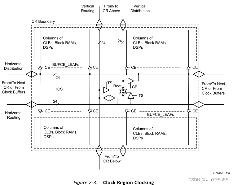
The clocks can be distributed from their sources in one of two ways (Figure 2-3):
时钟可以通过以下两种方式之一从其源进行分配(图 2-3):
-
The clocks can go onto routing tracks that take the clocks to a central point in a CR without going to any loads. The clocks can then drive the distribution tracks unidirectionally from which the clock networks fan out. In this way, the clock buffers can drive to a specific point in the CRs from which the clock buffers travel vertically and then horizontally on the distribution tracks to drive the clocking points. The clocking points are driven via leaf clocks with clock enable (CE) in that CR and adjacent CRs, if needed. Distribution tracks cannot drive routing tracks.
-
时钟可以进入布线轨道,将时钟带到 CR 中的中心点,而不需要任何负载。然后,时钟可以单向驱动分配轨道,时钟网络从该分布轨道扇出。以这种方式,时钟缓冲器可以驱动到CR中的特定点,时钟缓冲器从该点在分配轨道上垂直行进,然后水平行进以驱动时钟点。如果需要,时钟点通过该 CR 和相邻 CR 中具有时钟使能 (CE) 的叶时钟驱动。分配轨道不能驱动布线轨道。
-
This distribution scheme is used to move the root for all the loads to be at a specific location for improved, localized skew. Furthermore, both routing and distribution tracks can drive into horizontally or vertically adjacent CRs in a segmented fashion. Routing tracks can drive both routing and distribution tracks in the adjacent CRs while the distribution tracks can drive other horizontal distribution tracks in adjacent CRs. The CR boundary segmentation allows construction of either truly global, device-wide clock networks or more local clock networks of variable sizes by reusing clocking tracks.
-
该分配方案用于将所有负载的根移动到特定位置,以改善局部偏斜。此外,布线和分配轨道都可以分段方式驱动到水平或垂直相邻的CR。布线轨道可以驱动相邻CR中的布线轨道和分配轨道两者,而分配轨道可以驱动相邻CR中的其他水平分配轨道。 CR 边界分段允许通过重用时钟轨道来构建真正的全局、设备范围的时钟网络或更多可变大小的本地时钟网络。
-
Alternatively, clock buffers can drive straight onto the distribution tracks and distribute
the clock in that manner. This reduces the clock insertion delay. -
或者,时钟缓冲器可以直接驱动到分配轨道上并以这种方式分配时钟。这减少了时钟插入延迟。

-
Each of the four bytes in the XIPHY BITSLICE have six connections from the HCS to their
global clocking pins. Therefore, only six BUFGs can drive the BITSLICE clocking pins in
either half of an I/O bank (a maximum of 6 clocks can drive any half of an I/O bank). -
XIPHY BITSLICE 中的四个字节中的每个字节都有六个从 HCS 到其全局时钟引脚的连接。因此,只有 6 个 BUFG 可以驱动 I/O 组任意一半中的 BITSLICE 时钟引脚(最多 6 个时钟可以驱动 I/O 组的任意一半)。
本文来自互联网用户投稿,该文观点仅代表作者本人,不代表本站立场。本站仅提供信息存储空间服务,不拥有所有权,不承担相关法律责任。 如若内容造成侵权/违法违规/事实不符,请联系我的编程经验分享网邮箱:chenni525@qq.com进行投诉反馈,一经查实,立即删除!
- Python教程
- 深入理解 MySQL 中的 HAVING 关键字和聚合函数
- Qt之QChar编码(1)
- MyBatis入门基础篇
- 用Python脚本实现FFmpeg批量转换
- C# 操作非持久化内存映射文件
- Unity向量叉乘
- MATLAB算法实战应用案例精讲-【数模应用】匈牙利算法(Kuhn-Munkres)(补充篇)(附C语言代码实现)
- 十款强大的企业电脑加密软件推荐(企业电脑加密软件哪个最好用)
- UI功能6大流程、接口测试8大流程这些你真的全会了吗?
- 【TES720D-KIT】基于国内某厂商FMQL20S400全国产化ARM开发套件(核心板+底板)
- 可视化试题(一)
- Excel的COUNTIF的用法,用于统计重复值、满足条件值
- C-控制台-贪吃蛇
- 51单片机三种编译模式的相互关系