# 由cmos到基本逻辑门
由cmos到基本逻辑门
cmos
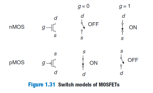
如图所示, g = 0 g=0 g=0时,p管连通,n管断开;否则相反。
Not gate

p p p管在上, n n n管在下;当 A = 1 A=1 A=1, p p p断开, n n n接通, Y Y Y输出GND,即为0。否则 Y Y Y输出 V D D V_{DD} VDD?,即为1。
NAND gate

p p p管并联, n n n管串联;根据与非的逻辑, A , B A,B A,B只要有任何一个为0,就会输出1;只有全1,才会输出0。
NOR gate

p p p管串联, n n n管并联;根据或非的逻辑, A , B A,B A,B只要有任何一个为1,就会输出0;只有全0,才会输出1。
参考资料
[1] Digital Design and Computer Architecture RISC-V Edition by Sarah Harris, David Harris
本文来自互联网用户投稿,该文观点仅代表作者本人,不代表本站立场。本站仅提供信息存储空间服务,不拥有所有权,不承担相关法律责任。 如若内容造成侵权/违法违规/事实不符,请联系我的编程经验分享网邮箱:chenni525@qq.com进行投诉反馈,一经查实,立即删除!
- Python教程
- 深入理解 MySQL 中的 HAVING 关键字和聚合函数
- Qt之QChar编码(1)
- MyBatis入门基础篇
- 用Python脚本实现FFmpeg批量转换
- 【工作流Activiti】MyActivit的maven项目
- 实习知识整理14:确认从购物车中下单的订单信息并实现相关的逻辑处理
- 【动态代理详解】
- Python大数据之Python进阶(七)线程的注意点
- nodejs如何使用clusster配置多cpu
- Redis(四)
- 磁盘阵列(RAID)
- Linux系统用户账号的管理
- 关于负载均衡器您需要了解和执行的所有操作
- 毕业设计——基于JavaEE采用MVC模式结合SSM框架进行实现,小区物业管理系统