Universal asynchronous receiver transmitter (UART)
UART Introduction
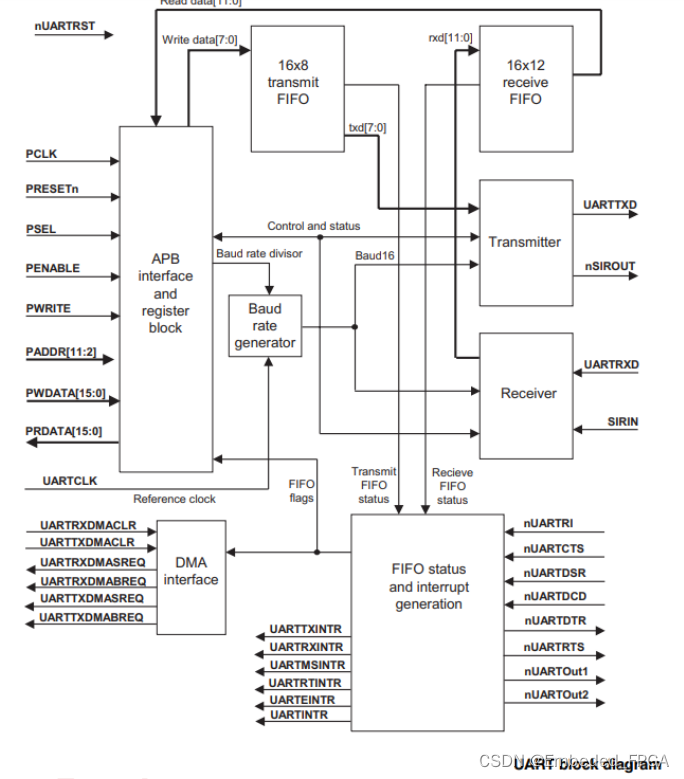
The UART is an AMBA slave module that connects to the Advanced Peripheral Bus (APB).
The UART (UART0 - UART4) are used to translate data between parallel and serial interfaces, provides a flexible full duplex data exchange using asynchronous transfer. It is also commonly used for RS-232 standard communication.
The UART includes a programmable baud rate generator which is capable of dividing the system clock to produce a dedicated clock for the UART transmitter and receiver. The UART also supports DMA
function for high speed data communication except UART4.
Programmable parameters
The following key parameters are programmable:
? communication baud rate, integer, and fractional parts
? number of data bits
? number of stop bits
? parity mode
? FIFO enable (16 deep) or disable (1 deep)
? FIFO trigger levels selectable between 1/8, 1/4, 1/2, 3/4, and 7/8.
? internal nominal 1.8432MHz clock frequency (1.42–2.12MHz) to generate low-power mode shorter
bit duration
? hardware flow control.
Additional test registers and modes are implemented for integration testing.
UART functional description
The UART performs:
? serial-to-parallel conversion on data received from a peripheral device
? parallel-to-serial conversion on data transmitted to the peripheral device.
The CPU reads and writes data and control/status information through the AMBA APB interface. The transmit and receive paths are buffered with internal FIFO memories enabling up to 16-bytes to be stored independently in both transmit and receive modes.
The UART:
? includes a programmable baud rate generator that generates a common transmit and receive
internal clock from the UART internal reference clock input, UARTCLK
221 / 306
? offers similar functionality to the industry-standard 16C550 UART device
? supports baud rates of up to 460.8Kbits/s, subject to UARTCLK reference clock frequency
The UART operation and baud rate values are controlled by the line control register (UARTLCR_H) and the baud rate divisor registers (UARTIBRD and UARTFBRD).
The UART can generate:
?individually-maskable interrupts from the receive (including timeout), transmit, modem status and error conditions
? a single combined interrupt so that the output is asserted if any of the individual interrupts are
asserted, and unmasked
? DMA request signals for interfacing with a Direct Memory Access (DMA) controller
If a framing, parity, or break error occurs during reception, the appropriate error bit is set, and is stored in the FIFO. If an overrun condition occurs, the overrun register bit is set immediately and FIFO data is prevented from being overwritten.
You can program the FIFOs to be 1-byte deep providing a conventional double-buffered UART interface.
The modem status input signals Clear To Send (CTS), Data Carrier Detect (DCD), Data Set Ready
(DSR), and Ring Indicator (RI) are supported. The output modem control lines, Request To Send (RTS), and Data Terminal Ready (DTR) are also supported.
There is a programmable hardware flow control feature that uses the nUARTCTS input and the nUARTRTS output to automatically control the serial data flow.

Interface reset
The UART are reset by the global reset signal PRESETn and a block-specific reset signal nUARTRST.
An external reset controller must use PRESETn to assert nUARTRST
synchronously to UARTCLK. PRESETn must be asserted LOW for a period long enough to reset the slowest block in the on-chip system, and then be taken HIGH again. The UART requires PRESETn to be asserted LOW for at least one period of PCLK.
18.3.2 Clock signals
The frequency selected for UARTCLK must accommodate the desired range of baud rates:
FUARTCLK (min) >= 16 x baud_rate (max)
FUARTCLK (max) <= 16 x 65535 x baud_rate (min)
For example, for a range of baud rates from 110 baud to 460800 baud the UARTCLK frequency must be within the range 7.3728MHz to 115MHz.
The frequency of UARTCLK must also be within the required error limits for all baud rates to be used.
There is also a constraint on the ratio of clock frequencies for PCLK to UARTCLK. The frequency of UARTCLK must be no more than 5/3 times faster than the frequency of PCLK:
FUARTCLK <= 5/3 x FPCLK
This allows sufficient time to write the received data to the receive FIFO.
18.3.3 UART operation
Control data is written to the UART line control register, UARTLCR_H. This register is 29 bits wide internally, but is externally accessed through the AMBA APB bus by three writes to register locations,
UARTLCR_H, UARTIBRD, and UARTFBRD. UARTLCR_H defines:
? transmission parameters
? word length
? buffer mode
? number of transmitted stop bits
? parity mode
? break generation.
UARTIBRD and UARTFBRD together define the baud rate divisor
Fractional baud rate divider
The baud rate divisor is a 22-bit number consisting of a 16-bit integer and a 6-bit fractional part. This is used by the baud rate generator to determine the bit period. The fractional baud rate divider enables
the use of any clock with a frequency >3.6864MHz to act as UARTCLK, while it is still possible to generate all the standard baud rates.
The 16-bit integer is loaded through the UARTIBRD register. The 6-bit fractional part is loaded into the UARTFBRD register. The Baud Rate Divisor has the following relationship to UARTCLK:
Baud Rate Divisor = UARTCLK/(16xBaud Rate) = BRDI + BRDF
where BRDI
is the integer part and BRDF is the fractional part separated by a decimal point as shown in
Figure below.

Figure: Baud rate divisor
You can calculate the 6-bit number (m) by taking the fractional part of the required baud rate divisor and multiplying it by 64 (that is, 2n, where n is the width of the UARTFBRD register) and adding 0.5 to
account for rounding errors:
m = integer(BRDF * 2n+ 0.5)
An internal clock enable signal, Baud16, is generated, and is a stream of one UARTCLK wide pulses with an average frequency of 16 times the desired baud rate. This signal is then divided by 16 to give
the transmit clock. A low number in the baud rate divisor gives a short bit period, and a high number in the baud rate divisor gives a long bit period.
Data transmission or reception
Data received or transmitted is stored in two 16-byte FIFOs, though the receive FIFO has an extra four bits per character for status information.
For transmission, data is written into the transmit FIFO. If the UART is enabled, it causes a data frame to start transmitting with the parameters indicated in UARTLCR_H. Data continues to be transmitted
until there is no data left in the transmit FIFO. The BUSY signal goes HIGH as soon as data is written to the transmit FIFO (that is, the FIFO is non-empty) and remains asserted HIGH while data is being transmitted. BUSY is negated only when the transmit FIFO is empty, and the last character has been transmitted from the shift register, including the stop bits. BUSY can be asserted HIGH even though the UART might no longer be enabled.
For each sample of data, three readings are taken and the majority value is kept. In the following paragraphs the middle sampling point is defined, and one sample is taken either side of it.
When the receiver is idle (UARTRXD continuously 1, in the marking state) and a LOW is detected on the data input (a start bit has been received), the receive counter, with the clock enabled by Baud16,
begins running and data is sampled on the eighth cycle of that counter in normal UART mode, or the fourth cycle of the counter in SIR mode to allow for the shorter logic 0 pulses (half way through a bit period).
The start bit is valid if UARTRXD is still LOW on the eighth cycle of Baud16, otherwise a false start bit is detected and it is ignored.
If the start bit was valid, successive data bits are sampled on every 16th cycle of Baud16 (that is, one bit period later) according to the programmed length of the data characters. The parity bit is then
checked if parity mode was enabled.
Lastly, a valid stop bit is confirmed if UARTRXD is HIGH, otherwise a framing error has occurred.
When a full word is received, the data is stored in the receive FIFO, with any error bits associated with that word.
Error bits
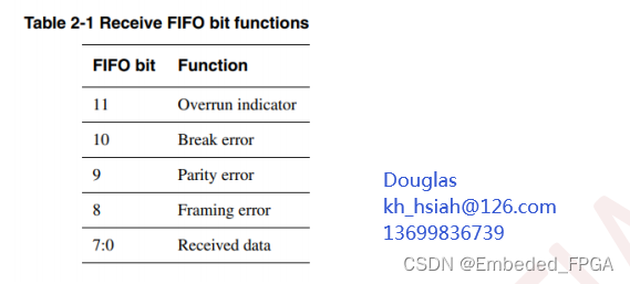
Three error bits are stored in bits [10:8] of the receive FIFO, and are associated with a particular character. There is an additional error that indicates an overrun error and this is stored in bit 11 of the receive FIFO.
Overrun bit
The overrun bit is not associated with the character in the receive FIFO. The overrun error is set when the FIFO is full, and the next character is completely received in the shift register. The data in the shift

register is overwritten, but it is not written into the FIFO. When an empty location is available in the receive FIFO, and another character is received, the state of the overrun bit is copied into the receive
FIFO along with the received character. The overrun state is then cleared. Table below shows the bit functions of the receive FIFO.
Disabling the FIFOs
Additionally, you can disable the FIFOs. In this case, the transmit and receive sides of the UART have 1-byte holding registers (the bottom entry of the FIFOs). The overrun bit is set when a word has been
received, and the previous one was not yet read. In this implementation, the FIFOs are not physically disabled, but the flags are manipulated to give the illusion of a 1-byte register. When the FIFOs are disabled, a write to the data register bypasses the holding register unless the transmit shift register is already in use.
System and diagnostic loopback testing
You can perform loopback testing for UART data by setting the Loop Back Enable (LBE) bit to 1 in the control register UARTCR (bit 7).
Data transmitted on UARTTXD is received on the UARTRXD input.
本文来自互联网用户投稿,该文观点仅代表作者本人,不代表本站立场。本站仅提供信息存储空间服务,不拥有所有权,不承担相关法律责任。 如若内容造成侵权/违法违规/事实不符,请联系我的编程经验分享网邮箱:chenni525@qq.com进行投诉反馈,一经查实,立即删除!